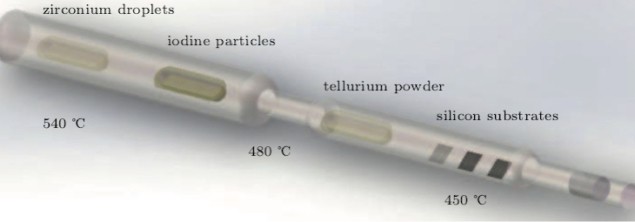
A supportive “mattress” of material has made it possible to grow nanoribbons of a previously hard-to-synthesize topological insulator. The technique, which is based on conventional chemical vapour transport, produces crystalline nanostructures of zirconium pentatelluride (ZrTe5) with a high carrier mobility, and could be used to produce ultrathin and even monolayer ZrTe5 in the future.
Topological insulators are materials that act as electrical insulators in their bulk, while conducting electricity extremely well on their surfaces (or edges) via special, topologically protected, electronic states. Within these states, electrons can only travel in one direction and do not backscatter. This remarkable behaviour allows the materials to carry electrical current with near-zero dissipation – meaning that they could someday be used to make electronic devices that are far more energy-efficient than any that exist today.
Even within this exotic family of materials, ZrTe5 stands out thanks to its wide variety of topological phases. Depending on how it is configured, it can behave as a weak or a strong insulator, a Dirac semimetal or a 3D quantum Hall state. When thinned down to a monolayer, it is also predicted to be a large band gap quantum spin Hall insulator.
Topological nanoribbons
Previous studies of ZrTe5 mainly focused on its 3D bulk form. For real-world applications, however, nanowires or nanoribbons may be more useful, as surface states play a more important role when the surface-to-volume ratio is higher. New electronic properties could also emerge. Research on other types of nanostructured topological insulators has already revealed unexpected phases, and novel phenomena called “Majorana zero modes” (which could be used as bits in quantum computers) were observed experimentally for the first time when indium antimonide (InSb) nanowires were combined with superconductors.
Until the present work, efforts to grow high-quality nanostructures of ZrTe5 had foundered for lack of a reliable way to produce them quickly or in large-enough quantities. The new technique developed by Xiaosong Wu and colleagues of Peking University and South University of Science and Technology of China in Shenzhen is based on conventional chemical vapour transport. Here, source materials such as zirconium and tellurium react in their gas phases with the help of a transport agent (iodine, in this case) and crystallize. “The only difference between our technique and the conventional method is the introduction of silicon, which allows for the growth of nanostructured ZrTe5,” Wu explains.
Silicon plays an important role in growth
The ZrTe5 nanostructures do not grow directly on the silicon substrate, Wu adds. Instead, they develop out of a “mattress” that mainly consists of Zr and Te in a ratio of around 1:3.
Wu thinks this ZrTe3 mattress may provide a more suitable substrate for ZrTe5 to grow on. Certainly, when he and his colleagues looked closer at the mattress’ edge, they observed etches in the silicon substrate. “We know that iodine reacts with silicon and forms SiI4, which is in the gaseous phase at the growth temperature we employed,” says Wu. “We found that silicon plays an important role in the reaction but we are as yet unsure on how it affects the growth process exactly.”

Tuneable superconductivity appears in topological insulator
The researchers say they can also grow millimetre-long single crystals in around two hours – a huge improvement on conventional methods, which require weeks.
Growing thinner nanostructures
According to the team, aberration-corrected transmission electron microscopy (TEM) images of the as-grown ZrTe5nanoribbons suggest that the structures are highly crystalline. Quantum transport measurements also show that they contain few impurities and that they have a high carrier mobility of over 30,000 cm2/Vs – meaning that they conduct electricity extremely well.
“Our method shows great promise for growing high-quality ultra-thin nanostructures of ZrTe5 and even monolayers,” Wu tells Physics World. “Being able to do so would allow us to make this large band gap quantum spin Hall insulator in the laboratory and study its fundamental physical properties in experiments.”
The researchers, who report their work in Chinese Physics B, say they are now busy improving their technique so they can grow thinner nanostructures.


