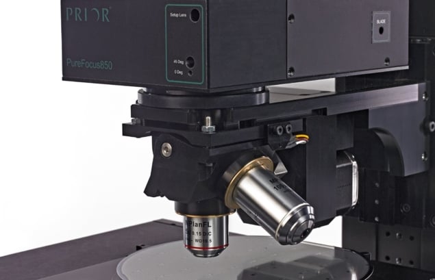
The PureFocus850 from Prior Scientific enhances the functionality of existing microscope systems by automatically recovering and maintaining focus during sample imaging

The PureFocus850 is a laser-based autofocus system that delivers enhanced imaging outcomes, sustained workflow efficiencies and reductions in capital spend across a range of applications in materials science, biological microscopy and industrial inspection. That’s the claim of Prior Scientific, a UK-based manufacturer specializing in the design and production of precision positioning devices, optical systems, automation solutions and microscope components.
The integrated autofocus unit – which comprises an infrared laser diode, precision optics, detector and on-board microcontroller – provides a real-time focusing capability for infinity-corrected optical systems and is suitable for both upright and inverted microscopes. “The PureFocus850 allows powerful autofocus functionality to be installed on the latest commercial microscopes or retrofitted as an upgrade to established imaging systems,” explains Simon Bush, sales engineer (UK and Ireland) at Prior Scientific. “The product is equally at home when integrated with a reflected-light optical system in a production-line context or when incorporated into an OEM imaging platform.”
In terms of operational specifics, the PureFocus850’s motorized offset lens adjusts the imaging depth into the sample, continuously holding the precise distance between imaging focal point and a reference boundary of choice. This capability can be put to work in all manner of imaging applications: from simply scanning across a biological sample on a slide without the need to manually refocus – yielding significant efficiencies for the user – to high-resolution tile-scanning or time-lapse imaging, where focus stability and accuracy determine the success of an experiment or sample analysis.
The commercial roadmap
Right now, Prior Scientific is busy developing several discrete customer segments for the PureFocus850. Within the research community, for example, the hardware autofocus offers scientists a cost-effective upgrade path for their existing microscope facilities, rather than recurring capital spend on new optical systems. A case study in this regard is the Nanofabrication Laboratory at Chalmers University in Gothenburg, Sweden, which required a retrofittable autofocus solution that will work with a variety of samples and objectives while ensuring compatibility with brightfield and darkfield imaging.

For a research facility like Chalmers, where a variety of experiments are run on the same microscope, other advantages include one-time installation and the ability of the PureFocus850 software to specify and store a range of autofocus settings (for example, laser power, recovery speed, focus stability and focus confirmation parameters). “We released an expanded range of inverted microscope kits at the end of 2020,” adds Bush, “and our aim is to cater for researchers who either require an out-of-the-box autofocus solution or one with an accessible SDK [software development kit] that can be used to develop a novel imaging system.”
Beyond the laboratory, the PureFocus850 provides a versatile option for specialist OEMs developing next-generation microscopy and imaging systems. There are several features – including extra-long-range recapture and interface detection – that are only accessible to OEM customers in a fully automated context, while the motorized offset has the potential to allow dynamic offset recalculation. The latter is paramount for ensuring focus stability over long periods when imaging different layers in multilayer samples, such as during laser scanning confocal microscopy (LSCM) or fluorescence-lifetime imaging microscopy (FLIM).
“The scope for modification is extensive,” notes Bush. “Customers can engage with our R&D team to change the optics, offset mechanics and laser wavelengths – for example, to support long-wavelength imaging such as two-photon microscopy or Raman spectroscopy. The autofocus also integrates with OpenStand, our instrument development platform for building OEM solutions and one-off customizations.”
Industrial inspection
Out in industry, meanwhile, the PureFocus850 has generated significant interest among customers engaged in low- to medium-throughput materials analysis and inspection. A case in point is Top-Electech, a China-based electronics supplier, which last year integrated the hardware autofocus into an existing microscope to fast-track the inspection and analysis of its PCB components – delivering a 95% reduction in processing time for multisample component arrays.
The PureFocus850 provides a neat fit for this application because it’s not tied to any particular software and can be used as a standalone microscope add-on or integrated into custom protocols via Prior Scientific’s SDK. What’s more, the technical challenges are non-trivial for the Top-Electech quality-assurance team, with electronic components first mounted in resin and then filed down to allow imaging of their internal structure – a process that creates a subtly uneven surface comprising materials with variable reflectance and contrast.
“Traditional software or hardware autofocus systems may struggle to maintain focus on this variable surface, but the PureFocus850 averages the signal reflected by the sample across the microscope’s field of view,” notes Bush. “This ‘line-mode’ capability allows a consistent, reliable signal to be obtained while scanning across each sample, even where parts of the field of view are non-reflective, ensuring the sample is constantly in focus without user intervention.”
Another issue is variation in the amount of light reflected by the sample depending on the magnification of the objective. As such, it helps that Top-Electech engineers can store the optimal laser power for each objective on the microscope to ensure seamless switching between high and low magnification while keeping the sample in focus. By also storing a sample detection threshold for each objective, the engineers are able to avoid large, unnecessary refocusing steps when moving between samples. This protective feature allows the loading of multiple samples onto the microscope simultaneously and the ability to image in sequence without the risk of refocusing onto areas of the microscope stage that do not contain a sample. “In this way,” notes Bush, “the Top-Electech team is able to undertake batch processing rather than loading and imaging samples sequentially.”
Elsewhere, STMicroelectronics, the multinational electronics and semiconductor manufacturer, has combined the PureFocus850 with image recognition software to automate the analysis of silicon-carbide wafers at its manufacturing facility in Sweden. The firm’s engineers use defect-selective etching to assess wafer quality – a process that creates etch pits on the silicon-carbide wafer surface, with the frequency, morphology and distribution of these pits linked to the type and location of potential defects within a sample. This uneven surface would typically cause problems for laser autofocus systems, but the line-mode configuration of the PureFocus850 uses a weighted average of the reflected signal to find the optimal focal plane.
In this use case, sample interrogation focuses on the bottom of the etch pits, such that the imaging plane of interest differs from the main reflective surface of the silicon-carbide wafer. “The analysis is enabled by the motorized optics of the PureFocus850, which allows the imaging plane to be offset from the wafer surface,” explains Bush. Equally important for STMicroelectronics is the efficient acquisition of brightfield and darkfield images, with the user interface allowing engineers to optimize the autofocus settings for each imaging technique based on the intensity of illumination and to easily switch between them (rather than having to find a compromise between the two).
“All told,” concludes Bush, “the PureFocus850 enables STMicroelectronics to acquire higher-quality tile-scans of their silicon-carbide wafers while delivering a massive improvement in throughput – typically an 85% reduction in the wafer scanning time.”


