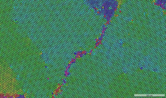
A new way of using self-assembling block copolymers (BCPs) to create patterned nanostructures has been unveiled by researchers in Canada. They found that arrays of BCPs with different lattice spacings can align preferentially to create well-defined moiré superstructures. These superstructures could be used to create optoelectronic devices that self-assemble, allowing device features to be much smaller than are currently possible using conventional fabrication techniques.
BCPs comprise two or more chemically distinct polymer chains connected via covalent bonds. By tuning the molecular weight, chemical composition and the volume fraction of the blocks, researchers can make BCPs that self-assemble into periodic nanopatterns such as arrays of parallel lines and hexagonal dot patterns on a variety of surfaces. Directed self-assembly (DSA) of BCPs by pre-defined templates could lead to patterning capabilities beyond the resolution limits of conventional optical lithography. This could result in components with feature sizes well below 20 nm for use in next-generation optoelectronics devices. Furthermore, the devices could have fewer defects and the process could be less expensive than conventional methods.
New field
DSA is a relatively new field of research and recently a team led by Erik Luber and Jillian Buriak at the University of Alberta and the National Research Council Canada used an array of hexagonal silica dots (prepared via BCP self-assembly) to direct the self-assembly of a second layer of the same BCP. The researchers converted the commensurate, two-layered pattern they produced to a honeycomb pattern of silicon dots that had double the density of the original dots. Now, the team has gone a step further and produced nanoscale structures using the DSA of two incommensurate BCP dot arrays.
“We did this by first depositing the bottom BCP layer as a thin film using a technique called spin coating, followed by solvent annealing to form a highly ordered hexagonal BCP lattice,” explains Luber. “We then converted this BCP lattice to an array of silica dots using reactive ion etching. We repeat this process on top of the same substrate using a different BCP with different lattice spacing. The alignment of the two layers is completely self-directed and is the result of energy minimization between the layers.”
Photonic metasurfaces
The researchers found that the layers align preferentially in a way that produces moiré superstructures – regular patterns created whenever two similar 2D lattices are overlaid – never seen before in DSA. These superstructures contain large, multi-micron-sized grains with preferred majority phases. “Although it is currently unclear what types of applications will make use of these BCP moiré superstructures, one promising application may be photonic metasurfaces with tuneable optical properties,” says Luber.
“We can modify the resultant moiré structure by not only changing the pitch ratio of the two dot lattices but also the dot height and size,” he explains. “We will now be exploring the effect of dot height while keeping all other parameters constant. This study should shed more light on how the moiré patterns form, and help us design these patterns in the future.”
The work is described in ACS Nano.
- A version of this article first appeared on nanotechweb.org


