Cell reproduction, disease detection and semiconductor optimization are just some of the areas of research that have exploited the atomic force microscope. First invented by Calvin Quate, Gerd Binnig and Christoph Gerber in the mid 1980s, atomic force microscopy (AFM) brought the atomic resolution recently achieved by the scanning tunnelling microscope to non-conducting samples, and helped to catalyse the avalanche of science and technology based on nanostructures that now permeates all aspects of modern life from smartphones to tennis rackets. On 6 July 2019 Calvin Quate died aged 95 at his home in Menlo Park, California.
Long before the development of AFM, Quate’s research had made waves in microscopy. 1978 had seen the announcement of the scanning acoustic microscope, which achieved the sensitivity of optical microscopy but probed samples so softly that it could image the interiors of living cells without damaging them. The technique uses high frequency sound waves in place of light, which penetrate deep into structures to image internal structures non-destructively. It is widely used in quality control of electronic component assembly among other applications such as printed circuit boards and medical products.
Although I later focused on optical and nanophotonic techniques, my own brief foray into microscopy began with a Master’s project on atomic force microscopy. Later while celebrating 30 years of the atomic force microscope at IOP Publishing, I had the chance to visit co-inventor Christoph Gerber at his University in Basel, Switzerland. He described how the idea had emerged during the Oberlach workshop where the first successful images with the scanning tunnelling microscope were announced. “Gerd Binnig came up with the idea to measure interactive forces between the tip and the sample surface and maybe this could be done by introducing a cantilever with an integrated tip,” says Gerber. “We took it from there and designed and developed the first AFM based on the latest development of the STM.”

Atomic force microscopy goes 3D
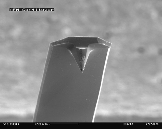
While scanning tunnelling microscopy uses tunnelling electronic currents to image the surfaces of conducting samples, AFM uses an atomic sharp tip attached to a cantilever that gently feels the topography as it scans in a similar way to the stylus of a record player. “When we published the paper in ’86 obviously lots of people picked up on it because it seemed to be so easy at the time just to scratch the surface with a stylus incorporated on a cantilever to get atomic resolution,” says Gerber. He describes how the first atomic resolution with the AFM was with a development from Quate’s group at Stanford University. “Calvin Quate had some extremely talented young pre-docs and postdocs and they developed the first cantilever from silicon, so this was batch microfabrication. It didn’t have a tip at that time – an integrated tip – but we were able to get the first atomic resolution on graphite just with the edge of that cantilever.”
One of Quate’s students Sang-Il Park went on to establish a successful business in atomic force microscopes at Park Systems. I had the chance to visit their labs too a few years ago, in Seoul, South Korea, where the company continues to push the capabilities of the technology.
The Leland T Edwards Professor of Engineering, emeritus, and a professor of applied physics at Stanford, Quate had accrued a panoply of awards over the course of his career, including the National Medal of Science, the Kavli Prize, the Rank Prize for Opto-Electronics and the Medal of Honor from the IEEE, as well as election to the National Academy of Engineering in 1970, the National Academy of Sciences in 1975 and Britain’s Royal Society in 1995. His legacy will continue for decades to come.
- This was edited on Monday 15th July 2019 to include reference to the legacy of Quate’s students.


