Light emitters made from 2D and quasi-2D materials are currently of great interest in nano-optoelectronics because their lack of dielectric screening means that their electron–hole pairs (excitons) are incredibly sensitive to their environment. This is advantageous for making devices such as highly responsive photosensors and electrochemical sensors.
When deposited directly onto the surface of a metal in a metal/dielectric substrate, the light emitted by these quasi-2D materials or “nano-emitters” can generate surface plasmon polaritons (SPPs). These are light–matter quasiparticles that exist at a metal/dielectric interface and propagate along it as a wave. An SPP is an electromagnetic wave (polariton) in the dielectric that is coupled to an oscillation of electric charge on the surface of the metal (surface plasmon). As a result, SPPs have properties that are similar to both matter and light.
The electromagnetic field of an SPP is confined to the near field. This means that it exists only at the metal/dielectric interface, with its intensity decaying exponentially with increasing distance into each medium. This results in a large enhancement of the electric field, making SPPs incredibly sensitive to their environment. What is more, near-field light can be manipulated at sub-wavelength length scales.
Until now, SPP/nano-emitter systems have been studied extensively in the optical far field, but the imaging techniques used are diffraction-limited and important sub-wavelength mechanisms cannot be visualized. In a new study described in Nature Communications, researchers in the US have used tip-enhanced nanospectrosopy to study SPPs in nano-emitters in the near field. This allowed the team to visualize spatial and spectral properties of the propagating SPPs. Indeed, their research could lead to exciting new practical plasmonic devices.
Bigger is not always better
In recent years, research into photonic devices and their integration into circuits has been of great interest in industry and academia. This is because compared to purely electronic devices, photonic devices can achieve higher energy efficiencies and faster operating speeds.
However, there are two big challenges that must be overcome before photonics overtakes electronics in mainstream applications. One is that purely photonic devices are difficult to connect together to form larger circuits; and the other is that the size of photonic devices cannot be made smaller than about half the wavelength of the light they process. The latter limits device sizes to about 500 nm, which is much larger than modern transistors.
Both of these problems can be solved by creating devices that operate using SPPs, rather than conventional light. This is because the light-like properties of SPPs allow for extremely fast device operation, whereas the matter-like properties of SPPs allow for easier integration into circuits and operation below the diffraction limit.
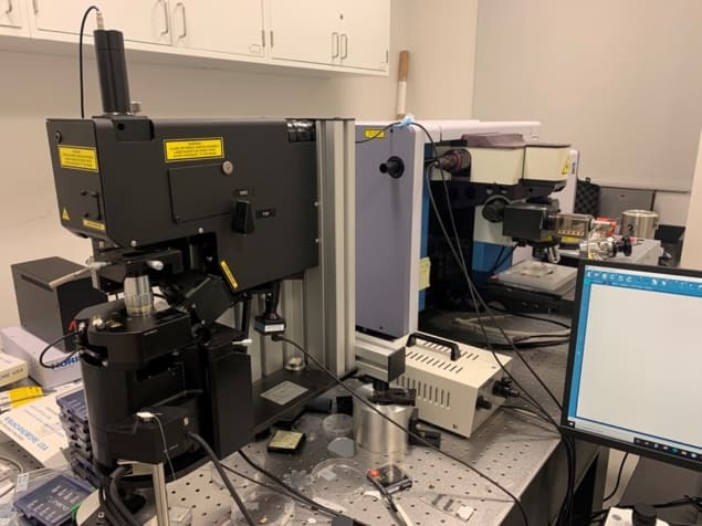
However, in order to design practical nano-electronics, a better understanding of the sub-wavelength behaviour of SPPs is needed. Now, Kiyoung Jo, a PhD student at the University of Pennsylvania, and colleagues have studied SPPs using tip-enhanced nanospectroscopy. This technique couples a far-field spectrometer with an atomic force microscope (AFM).

The gold-coated AFM tip scatters light in the near-field, which allows the SPPs to be spatially and spectrally imaged using the spectrometer. The sample was fabricated by spin-coating a solution of quasi-2D nanoplatelets (nanometre-scale flakes of the light emitter CdSe/CdxZn1-xS) onto an gold substrate and then depositing an aluminium oxide dielectric on top using atomic layer deposition.
The nanoplatelets were excited using a laser and their subsequent light emission launched SPPs that propagated along the gold/aluminium oxide interface. The researchers observed that the SPPs could propagate up to hundreds of microns and could also be reflected by the gold tip back along their original path. In case of reflections, the incident and reflected SPPs interfered with one another, forming a standing wave between the tip and the nanoplatelet (see figure: “Quasiparticle reflections”). Experimentally, these were observed as parabolic-shaped fringes.
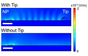
As the distance between the tip and the nanoplatelet was increased, the researchers found that the electric-field intensity varied periodically. This confirmed the presence of a standing wave and demonstrated how the nanoplatelet and tip act as a kind of cavity. Computer simulations showed, however, that, although both tip and nanoplatelet are required to observe fringes, the electromagnetic field generated by the SPPs is present with only one, confirming that both are able to launch SPPs.

Polariton condensation emerges from a bound state in the continuum
The researchers also investigated the effect of the sample properties on the SPP emission. For example, they found that fringes only occurred when the nanoplatelets were “edge-up” (perpendicular to the plane of the substrate), and the excitation laser was polarized such that its magnetic field was perpendicular to the plane of incidence (TM polarization). As a result the polarization of the excitation laser can be used as a “switch” to easily turn the SPPs on and off, which is an important feature for opto-electronic devices. The team also found that the shape of the fringes could be used to determine the dipole orientation of the nano-emitter, with the parabolic shape suggesting a slight incline (circular fringes would indicate an angle of exactly 90° to the plane of the substrate).
Thickness also played an important role in the properties of the SPPs, with thicker nanoplatelets yielding stronger electric fields, and thicker dielectrics resulting in longer SPP propagation distances. Studies using different dielectric materials (titanium dioxide; and monolayer tungsten diselenide) indicated that, due to increased electric-field confinement, a larger dielectric permittivity also resulted in longer propagation distances. This is important to know, as the propagation distance directly correlates to energy transfer by the SPPs. Jo summarizes that “We find, visualize and characterize the sub-wavelength-scale energy flow via SPPs in the vicinity of individual nanoscale emitters.”
The team has shown that tip-enhanced nanospectroscopy is a powerful tool for the study of the near-field in SPP systems, allowing various properties, such as dipole orientation and implications of sample design, to be determined. “The ability to image and examine sub-wavelength photonic phenomena in excitonic semiconductors makes [near-field scanning optical microscopy] a valuable tool for fundamental studies as well as semiconductor characterization,” says Deep Jariwala, who is corresponding author on the paper describing the work. Such an enhanced understanding of SPP systems will be invaluable in the development of practical nano-optoelectronic devices.


